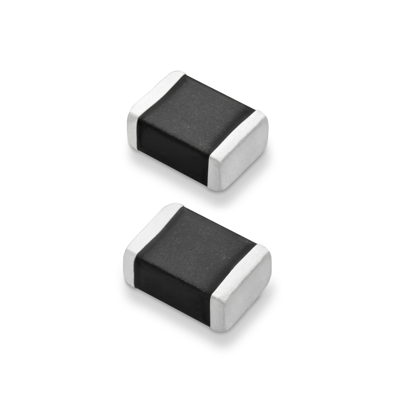

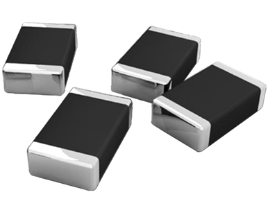
The CSPD family is a series of high-performance Chip Surge Protection Devices developed by SFI using advanced professional technologies.
CSPD exhibits excellent electrical characteristics including breakdown voltage, nonlinear α value, leakage current (Ir), and a tightly distributed capacitance with minimal deviation not only overcome the limitations of conventional market solutions such as gas discharge tubes (GDTs), metal oxide varistors (MOVs), and transient voltage suppressors (TVSs), but also offer superior protection performance.
With its ultra-low clamping voltage and rapid response time, CSPD provides enhanced protection and can withstand multiple surge current impacts.
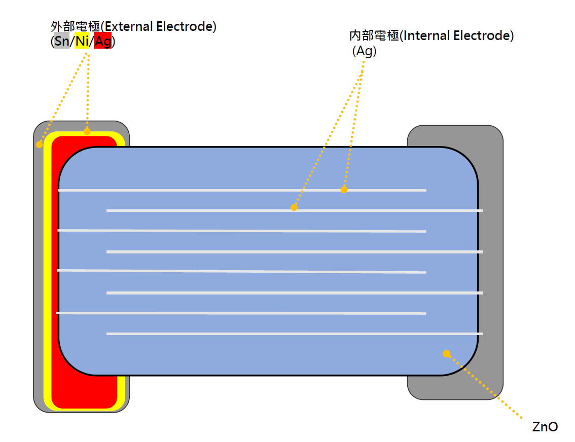
【Internal Structure】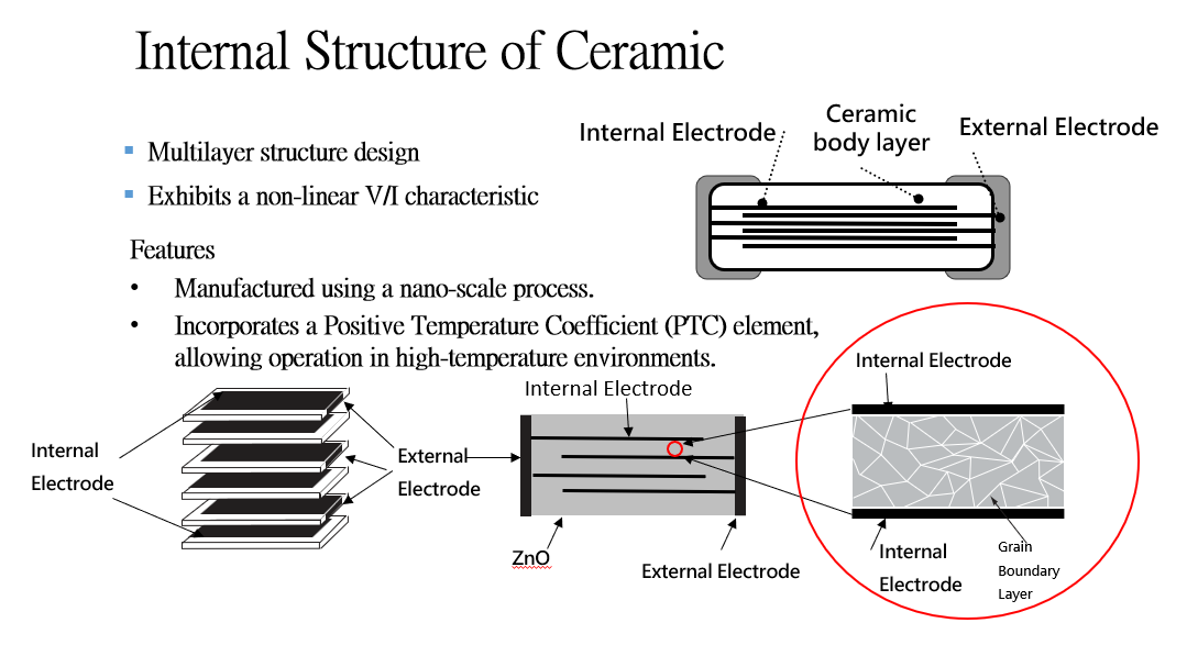
【Operating Principle】
SFI’s R&D center has pioneered an innovative approach to zinc oxide (ZnO) varistor material preparation. After more than five years of dedicated research, the scientific validity and commercial potential of this method were firmly established. This breakthrough led to the development of a wide range of high-performance ZnO ceramic materials many now in mass production under the CSPD series.
These materials not only meet but consistently exceed international standards. By utilizing low-temperature sintering, pure silver inner electrodes, and non-toxic solvents, SFI’s process significantly reduces environmental impact and minimizes the use of precious metals such as platinum and palladium:
- Introduction of a novel concept.
- Pioneered the world’s first use of low-temperature sintering with pure silver inner electrodes.
- Developed zinc oxide varistor ceramics with a high electric field gradient among the best globally.
- Achieved the highest surge current endurance in zinc oxide varistor ceramics worldwide.
- Engineered zinc oxide varistor ceramics for ultra-high temperature operation setting the global benchmark.
Reducing energy consumption, creating a green workplace, and protecting the global environment
【Features】
- Compact size with high energy capacity, ideal for high-density circuits
- Fast response to overvoltage events
- Capable of absorbing multiple surge pulses
- Low leakage current
- Bidirectional protection
- Excellent high-temperature performance
- Non-polarized design for easy PCB layout
- Easily scalable for mass production
- Batch-level testing ensures consistent quality
The SGD Family features a newly developed and innovative packaging technology using two PCBs (with internal routing) to extract wafer characteristics. These devices function as overvoltage protection components with performance equivalent to TVS, offering better surge current capacity and easier assembly.
SGD products are connected in parallel to electronic circuits for protection, and are commonly used in ESD protection for signal lines such as USB, HDMI, and RF interfaces, as well as in 3C products, industrial control systems, automotive communication, and medical electronics.
【Internal Structure】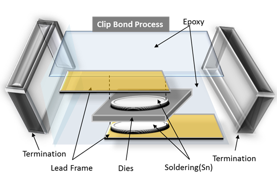
【Operating Principle】
SFI’s newly developed semiconductor packaging process for SGD replaces traditional wire bonding with a Clipper Bond (lead-free solder paste) surface contact method. This dramatically increases electrode contact area, improving surge current resistance, enhancing production yield, and reducing manufacturing time.
Using the same process, TVS diodes, switching diodes, and Schottky diodes can be surface-mounted (SMD), replacing traditional through-hole components. This allows space-saving designs that align with the trend toward thinner, lighter, and more compact systems.
【Key Features】
- Compact size with high energy handling—ideal for high-density circuits
- Fast overvoltage response
- Improved energy absorption through surface contact bonding instead of wire bonding
- Low leakage current
- Bidirectional protection
- Ultra-low capacitance
- Non-polarized design for easy PCB layout
- Suitable for mass production
- Batch-level inspection ensures consistent quality
- Wide variety of specifications available in different sizes, voltages, currents, and capacitance levels
Ideal for ESD protection in USB, HDMI, RF interfaces, as well as consumer electronics, automotive signal protection and more.